O Introduction
Laser particle size analyzer is the most advanced and most widely developed particle size measuring instrument. Its measurement principle is based on Mie scattering theory. Mie scattering theory is a classic light scattering theory. Its biggest feature is that it can be used to measure particles of any size, but its calculation is quite complicated, which limits the speed and accuracy of data processing.
DSP technology has many advantages to realize the MIE scattering algorithm: it is a dedicated CPU designed for algorithm calculation, so it has a fast calculation speed; it has a low cost compared to a general-purpose CPU, so it has a good price-performance ratio; and its small size , Can achieve the advantages of instrument integration and so on. ARM has abundant on-chip resources and is suitable for the development of embedded systems. It is mainly responsible for the operation of the operating system, task management and coordination, and DSP control tasks. .
1 Overall system design and working principle
1.1 Working principle of laser particle size analyzer

The photodetector in the laser particle size analyzer collects the scattered light of the particles in a certain angle range to obtain the particle size distribution information of the particles. Since the photodetector is on the focal plane of the Fourier lens, any point on the detector corresponds to a certain scattering angle. The photodetector array consists of a series of concentric annular belts. Each annular belt is an independent detector, which can linearly convert the scattered light projected onto it into a voltage, and then send it to the acquisition card. The card amplifies the electrical signal, then converts it to A / D and sends it to the computer. According to the program prepared in advance, the data processing is performed according to the Mie scattering theory, and the spatial distribution of the scattering spectrum is inverted into the particle size distribution.
1.2 The overall design of the circuit system
The overall block diagram of the laser particle size analyzer circuit is shown in Figure 2. The data collected by the acquisition circuit is transmitted to the DSP through the RS232 serial port, and after the operation of the DSP, the resulting data RS232 is transmitted to the ARM processor through the serial port, and the result is displayed on the touch screen interface of the ARM processor.

2 Specific design scheme of circuit system
2.1 Data acquisition circuit design
The photodetector of the particle size analyzer is made of a multi-element ring with a photocell. The multi-element ring photodetector receives the light energy of scattered light, and the ring-shaped photocell converts the light energy into photocurrent. Then through the current-voltage converter, the current signal is converted into a voltage signal. Then it is amplified by the amplifier circuit and then input to the A / D converter to convert the analog signal into a digital signal. Then the digital signal is input to the C805lF320 single-chip microcomputer, and the single-chip microcomputer is then transmitted to the DSP for processing, as shown in Figure 3.

The hardware components of the system are divided into the following parts: ring photodetector, data selection part, current-voltage conversion part, operation amplification part, analog-to-digital conversion part and central single-chip microcomputer control part.
â‘ The analog multiplexer uses ADG506, which has high precision, 1mV, strong anti-interference ability, low power consumption and cheap price;
â‘¡ The current-voltage conversion circuit has a capacitor and adjustable resistance that play a filtering role, which is helpful for adjusting the circuit parameters;
â‘¢ The cut-off frequency of the second-order Butterworth low-pass filter of the filter amplifier circuit is 10Hz, which mainly filters out the power frequency interference;
â‘£The chip used in the analog-to-digital conversion circuit is TLC2551, this chip is 14-bit A / D, the input voltage range is: O ~ 5V; the theoretical acquisition accuracy can reach 0.3mV, and the actual test accuracy can be limited to 0.8mV due to the actual test conditions ; A / D conversion time is 10m, and the acquisition speed is very high; this chip has strong anti-interference ability, low power consumption, and high cost performance;
⑤ The control circuit uses C8051F320 as the control chip of the acquisition circuit. It has abundant on-chip resources, the main frequency can reach 25MHz, and it is simple to develop and cost-effective. The data collected by the single chip microcomputer is sent to the DSP chip through the serial port.
2.2 Design of DSP arithmetic circuit
DSP is a kind of digital signal processor. Since its inception, DSP has been characterized by the stability, repeatability, and large-scale integration of digital devices, especially programmable and easy to implement adaptive processing. The development of signal processing has brought huge opportunities.
The data collected by the acquisition circuit of the laser particle size analyzer is transmitted to the DSP processor through the RS232 serial port, and the arithmetic operation is performed through the DSP. After the operation is completed, the data is transmitted to the embedded ARM processor through the RS232 serial port to display the results. The principle block diagram is shown in Figure 4 below:

â‘ DSP chip selects TMS320C5416, TMS320C5416 adopts improved Harvard structure, has the following advantages: with high parallelism and dedicated hardware multiplier and adder CPU design, chip performance is greatly improved; program memory and data memory are independent memories, each The memory is independently addressed and accessed independently. In this system, 16 data buses and 32 address buses are set, and the rest are control buses.
â‘¡The chip used for serial-to-parallel data conversion is TL16C752B. This chip has two serial port controllers, controller A and controller B. D00 to D07 are 8-bit data buses, and RXA and TXA and RXB and TXB are the data transmission port and data reception port of port A and port B, respectively. CSA and CSB are the chip select ports of port A and port B, respectively.
â‘¢RS232 level conversion circuit, the level conversion chip used is MAX3160 which converts the 3.3V TTL level to RS232 level.
2.3 Design of ARM display circuit
The S3C2440A developed by Samsung is an embedded microprocessor with ARM920T as the core. It has a maximum operating frequency of 433MHz and contains 3 channels of asynchronous serial ports, USB master and slave unit device interfaces, camera interface, touch LCD / TFT controller and many other on-chip peripheral interfaces. The LCD screen TD035STED2 is 3.5 inches, the screen resolution is 320 × 240, and can provide 262K medium colors.
2.4 PCB design
The design software used for PCB design is Protel99. The key to PCB design is: the analog circuit part should have good anti-interference ability and high reliability. The methods to improve the anti-interference ability of the circuit are: â‘ The layout of components should be reasonable; â‘¡ The wiring should be reasonable; â‘¢ The copper should be reasonable; â‘£ The metal shell should be grounded and shielded.
3 Analysis of experimental results
On the basis of completing the design of the circuit system, the laser particle size analyzer experiment is carried out. Under the conditions of the same environment, the same acquisition circuit and the same Mie algorithm, experiments were conducted with a standard P4 desktop computer and a DSP + ARM circuit. For the experimental sample, calcium carbonate with a particle size ranging from 0.1 to 100 μm that satisfies the RR unimodal distribution is used.
The above two methods were tested for 20 consecutive times. Compared with the standard sample, the measured d50 error is within ± 3%, the d10 and d90 errors are within ± 5%, and the repeatability is within ± 3%, indicating that the collection accuracy has reached the instrument standard. Experiments verify that the design of this system is at least 10s faster than standard P4 computer operation.
4 Conclusion
This article combines the high-speed processing capabilities of DSP and the management capabilities of ARM to give the entire system maximum flexibility in its structure. High-performance DSP can meet the needs of computing performance, and the controllability of ARM. Can solve the touch display collection results. At the same time, the volume of the instrument is reduced, and the calculation speed is improved.
| Certificate |
ISO14001, ISO18000, ISO9001 Certificate,
and GS certificate from TUV Company of Germany.
|
| Color | Various, according to your requirements |
| Materials |
A. Plastic parts: Imported LLDPE E. Outer cover: Soft Covering PVC
(Different material is available according to your needs)
|
| Advantage |
a.Anti-UV
b.Anti-static
c.Security
d.Environmental protection e.Uneasy to lose shape |
| Function |
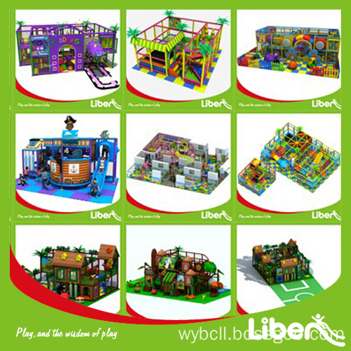
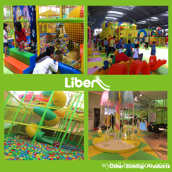
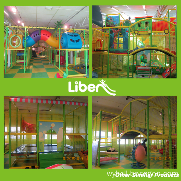
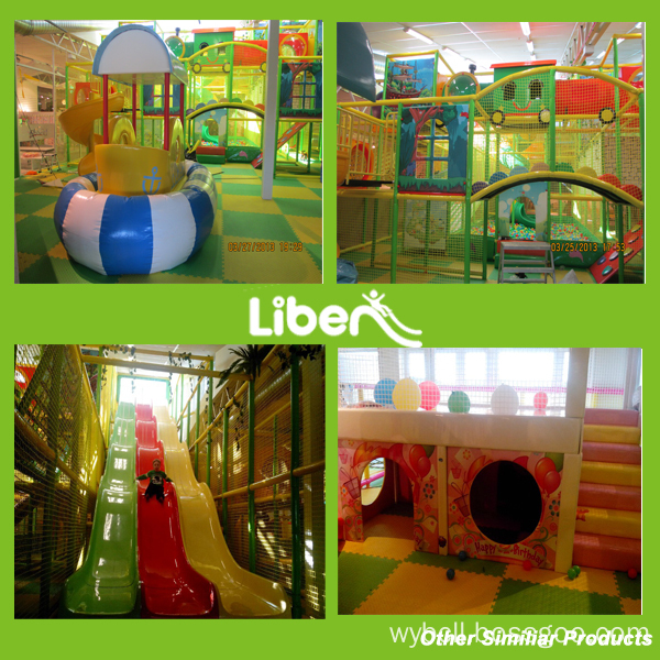
1.Can protect children safe when they playing indoor, and let they enjoy the play freely 2.Suitable for improving Children energy and imagination 3.Helping them grow up happily, cleverly, and healthily |
| Age Range | Children |
| Apply to | Amusement park, gymnasium, Kindergarten, Preschool, etc. |
| Packing | Standard export packing |
| Remark |
We can design and produce as your requirements |


Kids Soft Play, Soft Play Areas, Childrens Soft Play, Soft Play Centre
Liben Group Corporation , https://www.indoortrampoline.de